HDI PCB
HDI PCB Overview
In today’s rapidly advancing electronic technology, High Density Interconnect (HDI) PCB technology has become crucial for achieving the miniaturization and multifunctionality of electronic products. The design layout of HDI PCBs requires consideration of micro fine lines, small vias, and high-density components. These layouts significantly increase the integration of the circuit board, allowing electronic devices to perform more complex functions in smaller sizes.
The Role of HDI in PCBs
The high wiring density characteristic of HDI PCB technology has greatly promoted the development of compact electronic devices. By integrating more circuit components within a unit area, HDI PCBs significantly enhance the performance and functionality of electronic devices. This technology is particularly suitable for smartphones, portable medical devices, and high-end consumer electronics where space constraints are critical. Additionally, the use of blind and buried vias in HDI PCBs optimizes signal transmission paths, improves signal integrity, and reduces interference, which is crucial for high-speed data transmission and high-frequency applications.
Main applications include:
- Smartphones and tablets
- AI servers
- Automotive electronics
- Smartwatches
- Wearable medical devices
- Industrial Internet of Things
- Navigation flight control systems
HDI PCB Layout Design
During the HDI PCB design phase, several key aspects need to be considered comprehensively:
Component Placement: Designers must carefully consider the physical specifications, electrical performance, and thermal management requirements of components to ensure accurate and appropriate placement on the circuit board. This includes maintaining proper distances between heat dissipation channels and heat-sensitive components, as well as meeting Electromagnetic Compatibility (EMC) requirements.
Routing Planning: To optimize circuit performance, designers must carefully plan routing paths. This involves creating the shortest and most direct wiring connections while avoiding potential signal interference sources, such as power lines or high-speed signal paths, to reduce noise and transmission delays.
Via Design: As the bridge connecting different circuit board layers, the design accuracy of vias is crucial for ensuring signal integrity. In HDI PCBs, the size and position of vias need precise control to achieve accurate alignment between different layers and reliable electrical connections.
Layer Count and Stackup Structure: HDI PCBs may include multiple layers, such as 4, 6, 8, or more, to achieve the required circuit complexity and performance. Each layer’s design requires meticulous planning to ensure overall electrical performance and mechanical stability. This includes selecting appropriate insulating materials, determining the thickness of each layer, and deciding on the connection methods between layers.
8-layer Two Build-up HDI PCB Board
Material Type: HDI Blind and Buried Via Board Layer Count: 8 layers Board Thickness: 1.6mm Surface Finish: Gold Plating Minimum Line Width/Spacing: 3/3 mil
8-layer One Build-up Communication
HDI PCB Board
Material Type: HDI Blind and Buried Via Board Layer Count: 8 layers Board Thickness: 1.2mm Surface Treatment: Gold Plating + OSP (Organic Solderability Preservative) Minimum Line Width/Spacing: 3/3 mil
4-layer
HDI Rigid-Flex Board
Material Type: HDI Blind and Buried Via Board Layer Count: 4 layers Board Thickness: 0.8mm Surface Finish: Immersion Gold Minimum Line Width/Spacing: 3mil/3mil
The HDI PCB manufacturing process includes multiple steps, each requiring precise control:
- Material Preparation: Select appropriate substrate materials and copper foil to meet electrical and mechanical property requirements.
- Inner Layer Fabrication: Print circuit patterns on the substrate and perform etching to form the inner layer circuit.
- Lamination: Laminate the inner layers with other insulating material layers to form a multilayer board structure.
- Drilling and Plating: Drill holes in the PCB and then plate them with metal to form vias and conductive paths that connect different layers.
- Outer Layer Fabrication: Print the outer layer circuit on the laminated board and perform etching.
- Testing and Inspection: Perform electrical testing and visual inspection on the completed PCB to ensure its performance meets design requirements.
Quick Turn
Overview of the Design and Manufacturing Process for HDI (High-Density Interconnect) PCBs:
Determine the Number of Layers: First, determine the number of layers required to route all signals. This can be achieved by using the largest BGA component on the board or the interface and direction count of the largest IC on the board.
Select Materials: Contact your manufacturer to select materials and obtain dielectric data to create your PCB stack-up.
Determine Via Patterns: Based on the number of layers and thickness, determine the via patterns used to route signals through the inner layers.
Conduct Reliability Assessment: If relevant, conduct a reliability assessment to verify that the materials will not cause stress-induced fractures in the interconnections during assembly and operation.
Define Design Rules: Define design rules based on the manufacturer’s capabilities and reliability requirements (such as teardrops, trace width, spacing, etc.) to ensure reliable manufacturing and assembly.
Stack-Up Creation and Design Rules: The creation of the stack-up and the determination of design rules are critical points as they will determine the routing capability of the board and the reliability of the final product. Once these steps are completed, designers can implement the manufacturer’s DFM (Design for Manufacturing) and reliability requirements as design rules in the ECAD software. Performing this at the front end is crucial as it will help ensure the design is reliable, routable, and manufacturable.
Design Feature Sizes to Meet HDI DFM Requirements
Despite the stringent DFM requirements related to HDI PCB spacing, these requirements can be met by utilizing design rules in PCB design software. Some important DFM requirements to gather before layout and routing include:
- Trace width and spacing limits
- Annular ring and aspect ratio limits, especially for high-reliability designs
- Material systems used in the board to ensure controlled impedance in the required stack-up
- Impedance curves for the required stack-up or layer pairs (if available)
Design tools are crucial for designing HDI boards to meet these DFM requirements. Using the right design tools, routing impedance-controlled traces in HDI PCBs is very easy. You simply need to create an impedance profile and define the required trace width while keeping the manufacturer’s DFM guidelines in mind. The online DRC (Design Rule Check) engine in the routing software will check the routing as you create the HDI layout. Ensure you obtain a complete set of specifications for the manufacturer’s process to ensure you have considered all relevant HDI DFM rules.
Types of Vias in HDI PCB Routing
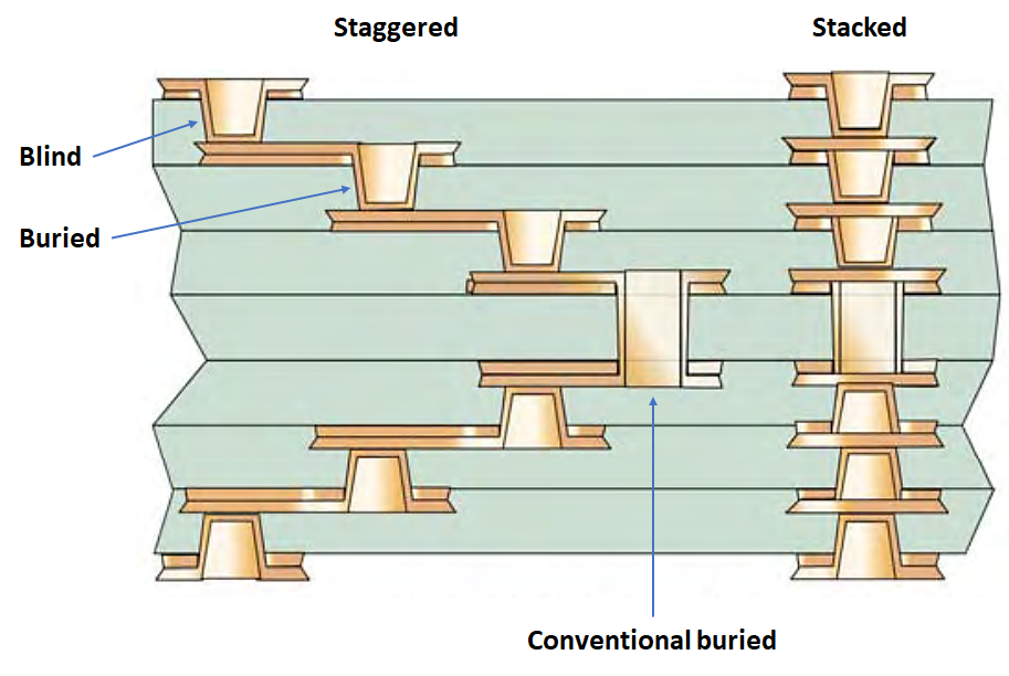
The image below shows typical via styles used in HDI PCB layout and routing. These via styles generally have a low aspect ratio (ideally less than 1), but some manufacturers may provide reliability statements for aspect ratios up to 2, including stacked microvias. At the center of the PCB stack-up is a traditional buried via, which provides connections through the thicker core layers; this inner-layer buried via can have a higher aspect ratio since it will be mechanically drilled.
After determining the number of layers and dielectric thickness, designers can design the vias according to the aspect ratio limits listed above. Adhering to the aspect ratio limits for microvias is crucial for reliability, especially when these boards undergo reflow or are deployed in environments subject to repeated thermal/mechanical shock and cycling.
Sequential Lamination Process
The sequential lamination process is primarily used to build HDI stack-ups layer by layer. Generally, this technique can be applied to any multilayer PCB, but it is especially important for HDI. This is because high-density, very thin dielectrics are formed in various layers around a thick core, so lamination will be performed in multiple steps to build the stack-up. The sequential lamination process includes the following steps:
- Photoresist Deposition and Exposure: Used to define the areas to be etched, leaving a conductor pattern on the laminate.
- Etching and Cleaning: The industry-standard etchant is ferric chloride solution. After etching, the remaining photoresist can be stripped, and the resulting conductor pattern is cleaned.
- Via Formation and Drilling: Vias need to be defined using mechanical or laser drilling. For high via density, chemical methods can be used to remove the vias.
- Via Metallization: Once the vias are defined, they are metallized to form continuous conductive interconnections.
- Construction: Before processing the outer layers, the layers are stacked through multiple lamination cycles to build the stack-up structure.
A flowchart showing the construction process can be found in the metallization section below.
Via Formation in HDI
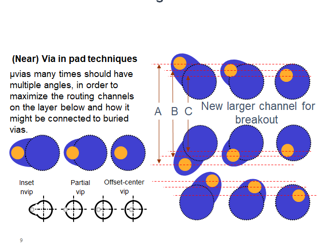
The interconnections required in HDI PCBs often reach the lower limit of via sizes that can be placed in a PCB through mechanical drilling. Once the via size is smaller than 6 mils, alternative via formation processes are needed to place microvias between layers. Since filled and plated microvias are a standard feature on HDI PCBs, they can be used in via-in-pad designs to help increase density. Using via-in-pad is a simple way to fit more components into the design, as they provide direct connections from component leads to internal layers.
Metallization
During the sequential lamination process, each layer in an HDI PCB undergoes via metallization, filling, and plating processes. The final vias in the internal structure must be void-free and have sufficient wrap plating around the neck to prevent cracking during reflow cycles and operation. There are four via metallization processes used in HDI manufacturing:
- Conventional Electroless Copper and Electroplated Copper
- Conventional Conductive Graphite or Other Polymers
- Full and Semi-Additive Electroless Copper
- Conductive Paste or Ink
Larger vias can be drilled, but due to the slower drilling speed, the cost eventually exceeds that of laser drilling, and the productivity is lower. Laser drilling is by far the most popular microvia formation process, but it is not the fastest. Chemical etching of small vias is the fastest, with an estimated speed of 8,000 to 12,000 vias per second. Plasma via formation and photovia formation are also fast.
Laser Drilling
In laser drilling, a high-energy density beam is used to drill holes in the PCB laminate. The laser can ablate dielectric materials and stop when it cuts through the copper circuit, making it ideal for creating depth-controlled blind vias. The laser energy wavelength is in the infrared and ultraviolet regions, with beam spot sizes as small as approximately 20 microns.
Microvia Manufacturing Techniques in HDI
If the vias on the board are wide enough to be drilled, controlled drilling steps can be used to place the vias. This requires intermediate sequential lamination steps to bond two layers of the board, followed by drilling and plating to define the via barrel, connections to inner layers, and landing pads on the upper layer. These vias may also be filled before the next sequential lamination step (if they are in the inner layers), or they can remain unfilled if they are on the outer layers. The overall drilling and sequential process is as follows:
- Intermediate Sequential Lamination: Bonding two layers of the board.
- Drilling and Plating: Defining the via barrel, connections to inner layers, and landing pads on the upper layer.
- Filling (if necessary): Filling the vias before the next sequential lamination step.

In Summary
HDI PCB manufacturers are crucial in the electronics industry. They produce high-density interconnect (HDI) PCBs, which are essential for compact and efficient devices. The HDI PCB manufacturing process involves advanced techniques like laser drilling and microvia technology. These manufacturers ensure high quality and reliability. Their expertise supports innovations in smartphones, medical devices, and automotive electronics. Choosing a reputable HDI PCB manufacturer guarantees superior performance and durability in your products.