What is Ceramic PCB
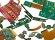
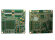
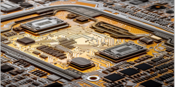
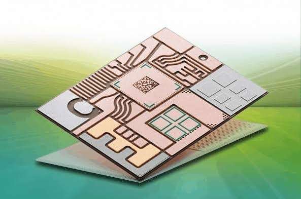
A Ceramic PCB, or Ceramic Printed Circuit Board, is a type of circuit board that utilizes ceramic materials for its substrate. Ceramics are renowned for their superior electrical insulation, mechanical strength, and thermal conductivity, which render them ideal for a wide array of applications. These properties not only ensure reliable performance but also contribute to the durability and longevity of the circuit boards in demanding environments.
Ceramic PCBs are employed in a variety of applications
where superior thermal management, high-frequency performance, and reliability are paramount. Here are some common uses:
High-Frequency Electronics: Ceramic PCBs are frequently utilized in RF (radio frequency) devices, microwave circuits, and radar systems. Their low signal loss and high dielectric constants make them well-suited for these high-frequency applications.
LED Lighting: As substrates for LED modules, ceramic PCBs play a crucial role due to their efficient heat dissipation capabilities. This helps to preserve the longevity and performance of LED lights.
Power Electronics: In the realm of power electronics, where efficient heat dissipation is critical, ceramic PCBs can withstand high temperatures and offer thermal stability, making them an excellent choice.
Aerospace and Defense: These sectors rely on ceramic PCBs for their radar systems, communication equipment, and missile guidance systems. Their dependability and high-frequency capabilities are particularly valuable in these high-stakes applications.
Medical Devices: Certain medical devices, such as medical imaging equipment and wireless communication devices, benefit from the superior performance and durability provided by ceramic PCBs.
Ceramic PCBs are manufactured through a series of specific and intricate processes that leverage the unique properties of ceramic materials. Here is an overview of the key manufacturing processes involved in creating ceramic PCBs, tailored to align with the standards of European and American readers:
Material Selection: The process begins with selecting the appropriate ceramic material for the substrate. Common choices include Alumina (Al2O3), Aluminum Nitride (AlN), Beryllium Oxide (BeO), Low-Temperature Co-fired Ceramic (LTCC), and High-Temperature Co-fired Ceramic (HTCC) .
Substrate Preparation: Once the ceramic material is chosen, the substrate is prepared. This involves cutting the ceramic substrate to the desired size and shape, grinding and polishing the surface for smoothness and flatness, and cleaning to remove any contaminants .
Via Formation: Vias are holes drilled through the ceramic substrate to create electrical connections between different layers of the PCB. This can be done through mechanical drilling with diamond-tipped drill bits or laser drilling, which uses a high-energy laser beam to ablate the ceramic material and create precise vias .
Metallization: This process involves depositing conductive metal layers onto the ceramic substrate and into the vias to form the circuit patterns. Metallization can be achieved through various methods, including screen printing of metal paste, sputtering, or electroless plating .
Patterning: After metallization, the conductive layers are patterned to create the desired circuit layout. This is typically done using photolithography and etching processes. A photoresist layer is applied, exposed to UV light through a photomask, developed, and the unwanted metal areas are etched away .
Lamination and Bonding: For multi-layer ceramic PCBs, individual layers are stacked and bonded together. This involves aligning the layers, applying a bonding material such as glass frit or adhesive, and laminating the layers under high pressure and temperature to form a cohesive structure .
Finishing and Quality Control: The final steps involve applying a protective and conductive surface finish, such as gold or nickel, to the exposed metal areas to prevent oxidation and improve solderability. The PCB is then tested for electrical continuity, insulation resistance, and other parameters to ensure functionality and reliability. Visual inspection for defects and packaging complete the manufacturing process